ABSTRACT
This paper highlights the critical production process parameters and necessary automated control to allow high yield on complex coatings. Material considerations, tooling, monitoring scheme, uniformity fluctuations with respect to substrate geometry and jig to source geometries are considered.
A range of complex coatings is described which illustrates the effects on coating performance of automated control of optical monitoring, distributed quartz crystal monitoring and substrate heating.
INTRODUCTION
Modern optical instrumentation inevitably requires optical multilayer coatings, such as anti-reflection coatings, laser mirrors, beam splitters, polarisers and dichroic filters1. A current example is the full scale implementation of optical telecommunications networks, generating needs for ultra-high precision filters for dense wavelength division multiplexing and gain flattening. Such optical multilayer systems often involve sophisticated designs for specialized filters, consisting of layers, which have thicknesses that bear no simple relationship to one another.
Usually these coatings are produced by vacuum evaporation of materials chosen with regard to refractive index, absorption, packing density, purity, susceptibility to water penetration and sticking coefficients. The material physical properties have an important role to play in determining achievable optical performance and long-term stability of filter characteristics.
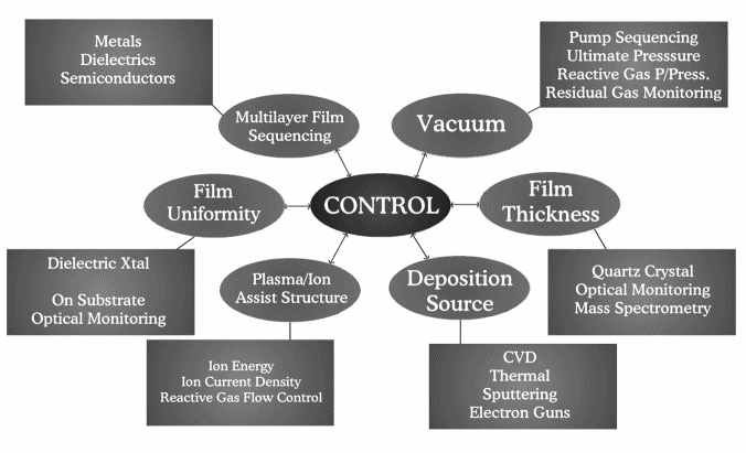
Reproducible filter properties, which match design expectations, are critically dependent upon accurate real-time control of a large number of parameters summarized in Figure 1. These include film thickness, condensation rate, plasma/ion assist control parameters and substrate temperature as well as the composition of the residual gas atmosphere. Currently available monitoring and control techniques for deposition systems provide control of these parameters, although not to the extent of error free multilayer structures.
Many of the control parameters are interdependent; therefore closed loop control is usually required. An example is the need to maintain constant deposition rate by controlling power delivered to the evaporation source.
Figure 1. Vacuum deposition control parameters
This paper will describe the effectiveness of two routinely used monitoring methods; quartz crystal and optical techniques, with associated limitations in achieving complex filter fabrication. These limitations in relation to variation of process parameters will be highlighted and use of automated control systems to minimise such variation described. Production of multilayer dielectric coatings requires maximum plant loading with high process yield and reproducibility. To this end, the coating production tolerance is a useful parameter in deciding appropriate monitoring schemes and the effects of process parameter variations on coating performance and yield.
Many previous reports(2-4) have described specific aspects of optical coating manufacture. Few have described the general consequences of all effects on manufacturability.
Use of a production tolerance concept is demonstrated to identify the degree of difficulty and therefore the degree of control that is required.
CONTROL AND COATING SYSTEM CONFIGURATION
This work refers to the production of particularly complex multilayer dielectric optical coatings. The work has been carried out in a diffusion pumped production box coater.
General configuration of the coating system is shown in Figure 2. The system incorporates two 14kW electron beam evaporation sources (low and high refractive index materials SiO2 and TiO2 respectively), optical and quartz crystal monitoring for thickness control and spatially distributed quartz crystals for monitoring the evaporant plume.
As the evaporation rate can be strongly influenced by the variable characteristics of the material5, optimal selection of electron gun configuration and operating conditions is key. Optimal evaporation characteristics of materials from electron guns have been well described eleswhere6.
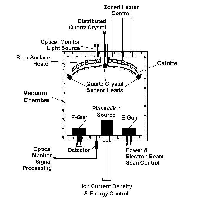
Figure 2. Coating system configuration.
The system also included front and rear surface substrate heating, capable of achieving 300°C substrate temperatures. The rear heaters are split into three spatial zones (shown as A, B and C in Figure 2). Film thickness and uniformity control is summarized in Figure 3.
The overall philosophy for the control system is centralized PC based co-ordination, as shown in Figure 1, and monitoring of each control sub-system (i.e. optical and quartz crystal monitoring, electron gun power and electron beam scan control etc). Centralized PC co-ordination of each control subsystem is through interfacing with local PC/PLC that provides necessary feedback control and data processing speed.
Other features of the control system are high reliability, ease of use, flexibility to adapt for production end-use and multi-level user access for production operation, process recipe definition and maintenance. To this end, the system utilizes well-proven hardware with a combination of PC and PLC control.
Automatic process control is based on tried and proven PLC hardware and software comprising a deposition controller and a vacuum management controller. The vacuum management controller automatically controls all aspects of system vacuum - valves, pumps, and hot/cold water feed to plant. The deposition controller and vacuum management controller combination is fully interfaced with the quartz crystal and optical thickness monitoring equipment.
A centralized PC-based touchscreen displaying a set of self-contained customized screens enables set-up and monitoring of all aspects of plant and process control. Real-time data logging of all aspects of the process is also provided.
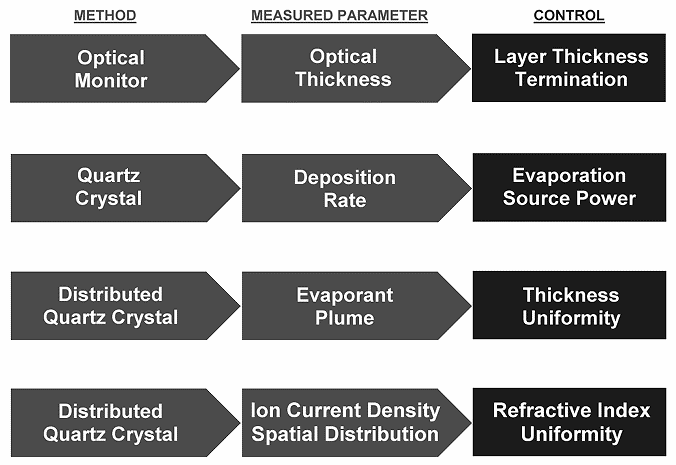
Figure 3. Film thickness and uniformity control.
The 'Recipe' screen contains all the essential parameters used for automatic execution of a deposition run with film values, tooling and gain set factors - presented in a spreadsheet format as standard - to enable quartz crystal control via the deposition controller. This system can handle 99 recipes of up to 250 layers each.
The 'Run' screen is used to display data corresponding to each of the deposition runs, collected via the data logger.
PRODUCTION TOLERANCE
In the preparation of complex multilayer optical coatings, it is useful to define a production tolerance. This value can be assigned to a particular coating design that identifies the degree of difficulty and therefore the degree of control that is required to successfully deposit the coating. The production tolerance can be defined in many ways depending on the particular application.
For edge filters and narrowband coatings, the optical specification usually calls for a wavelength location. It is therefore often sufficient to define the production tolerance for the wavelength location range as a percentage of the wavelength for which the edge or peak transmission meets the requirements of the specification.
Production tolerance = ±l/2w x 100%
where l is the wavelength range for coating within specification and w is the wavelength of feature. For example, if a specification called for a transmission of >50% at 694nm for a narrowband coating and the design had a bandwidth of 10nm, the production tolerance would be ±0.72%.
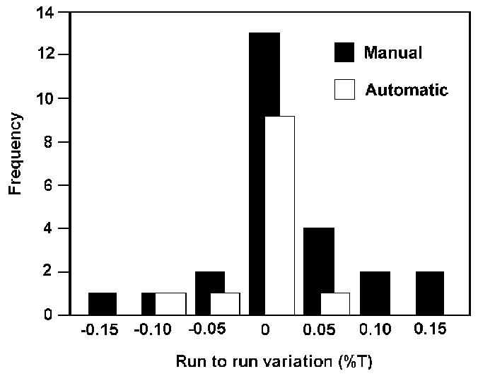
Figure 4. Optical monitoring repeatability for manual and automated layer termination control of a narrowband coating.
For other optical coating types where a specific transmission or reflection value is required, e.g. anti-reflection coatings, visual attenuator coatings and high reflectors, then another approach is required. An individual layer random error analysis can be performed to identify the allowable layer thickness and index variations. This then allows a production tolerance to be identified and necessary process parameter control.
Once a production tolerance has been identified, a suitable manufacturing method can be found. There are many options, such as choice of materials, choice of monitoring scheme and choice of deposition conditions that must be compatible with plant capabilities and optical requirements. Each manufacturing method has associated errors, random errors, systematic errors and other known errors. In order to choose a manufacturing process for optical coatings with a high yield within specifications these errors have to be categorized and related to the production tolerance of each design.
Systematic errors can arise from many sources and have to be controlled with respect to the production tolerance. Systematic temperature rises can cause changes in the sticking coefficient of some materials and changes in refractive indices of others. Source tunneling causes systematic changes in material distribution at different parts of the jig relative to the monitoring position.
Known errors can arise from many sources and usually cannot be controlled. Uniformity aspects on curved substrates can only be accounted for in one direction with single rotation tooling. It is also known that there is poorer repeatability using quartz crystal monitoring as compared with optical monitoring.
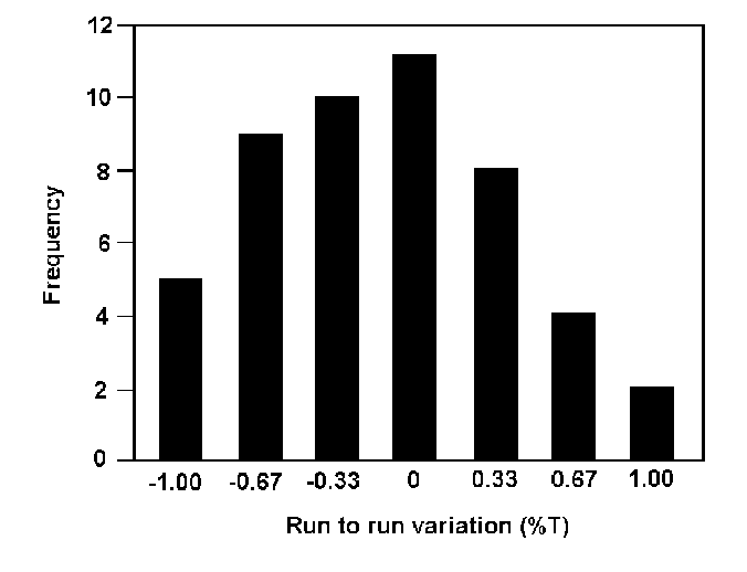
Figure 5. Quartz crystal monitoring repeatability. Based on the repeatability of a broadband 5-layer AR coating.
RESULTS AND DISCUSSION
Monitoring
In the manufacture of optical thin films, the choice is quartz crystal monitoring or optical monitoring for individual layer thickness determination. Optical monitoring provides a direct measurement of the optical thickness. However, it is not readily automated and is unsuitable for very thin layer deposition. Quartz crystal monitoring provides an indirect measurement of thickness and is consequently less accurate, however, it is suitable for both thin layer deposition and full automation.
Measurements of optical monitor performance during preparation of a narrowband coating have indicated that ± 0.15% run-to-run repeatability can be achieved (Figure 4). This was determined over twenty-four deposition runs for a narrowband 35-layer - (HL)42H(LH)4L(HL)42H(LH)4 - coating (H = TiO2 1/4w optical thickness, L = SiO2 1/4w optical thickness). Transmission was assessed on the optical monitor witness piece and therefore does not take into account other systematic errors.
Also shown in Figure 4 is the benefit of automated control using shape recognition algorithms for automated layer termination. In this case, run-to run repeatability is ±0.08%. Further improvement has been demonstrated by monitoring the rotating substrate directly, and combined with automated layer termination a run-to-run repeatability of ±0.04% is achievable.
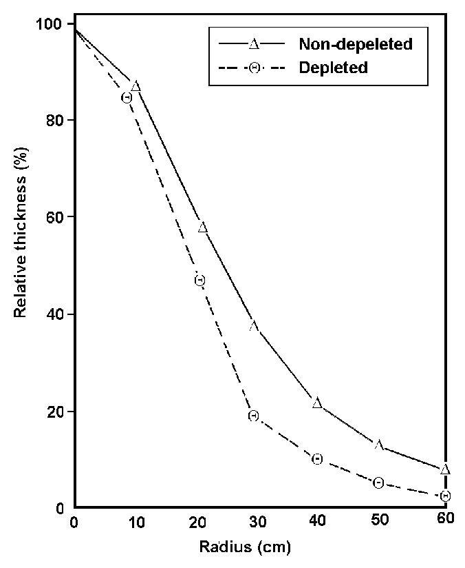
Figure 6. Relative SiO2 thickness distribution for non-depleted and depleted source material.
As accurate measurements cannot be made of film optical properties on quartz crystals, the assessment of quartz crystal monitoring repeatability is more difficult. To illustrate this aspect a broadband 5-layer anti-reflection TiO2/SiO2 multilayer coating, utilized for 1550nm laser diode end-facet ARCs, was chosen in order to minimize source-tunneling effects. A quartz crystal controller was used with automated control of layer termination.
The repeatability over 49 runs was measured on a rotating witness piece 30cm from the quartz crystal position. Although the measured run-to-run repeatability was ±1% (Figure 5) it is expected that other factors such as temperature fluctuations, reactive gas partial pressure fluctuations, and source geometry fluctuations would have contributed to this. A purely quartz crystal monitoring repeatability of approximately ±0.5% is therefore estimated.
Source fluctuations
An evaporation source can be thought of as a cosine emitter where source characteristics are given by the power of the cosine (Q-value)7.
Thickness =KcosQ a
where a is the angle at source and K is constant.
Generally, the more directional the source the greater the Q value. Figure 6 shows the flux distributions for electron beam evaporation of SiO2 at the start of a coating run and at a stage when material has been used up to an extent that electron beam source tunneling has occurred. This results in a more directional evaporant flux and hence a higher Q value. Materials with this problem are subliming and locally melting substances such as ZnS, SiO2, Ta2O5, Al2O3, Cr, etc. The variations in Q values depend specifically on electron beam source set up parameters and can, by careful set up, be minimized.
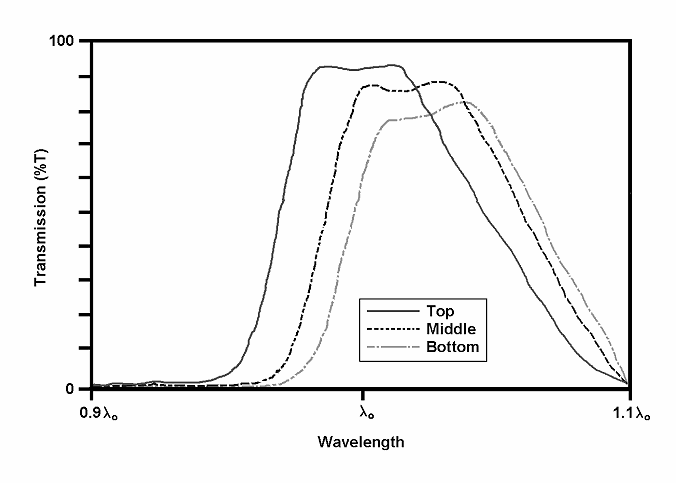
Figure 7. Measured transmission of bandpass filters at the top, middle and bottom positions of a rotating calotte prepared with no correction applied to depleting SiO2 electron beam source.
Electron gun placement on the baseplate, evaporant throw distance and method of substrate movement must be selected to maximize thickness uniformity and also minimize optical anisotropy effects8.
Typical values would, however, be Q = 1.5 for a newly replenished SiO2 source rising to Q = 2.0 for a used SiO2 source. These values can then be put in a thin film uniformity prediction program to determine the systematic shift in film thickness expected during coating deposition across the calotte. The example is shown for two measured band pass filters prepared with a Si02 electron source corrected and not corrected to minimize material tunneling (Figures 7 and 8, respectively).
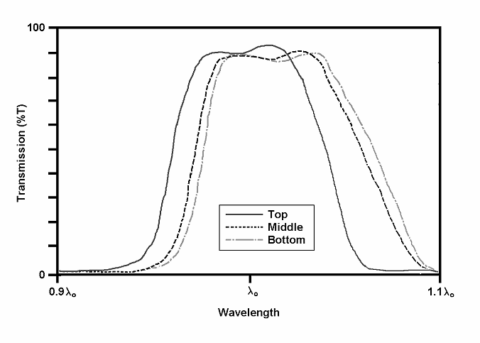
Figure 8. Measured transmission of bandpass filters at the top, middle and bottom positions of a rotating calotte, corrections applied to electron beam seem to minimize tunneling of SiO2 source. Only wavelength location errors are present.
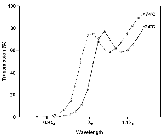
Figure 9. Spectral transmission of a multilayer edge filter at room and elevated temperature.
Distributed quartz crystal monitoring provides a means of real-time measurement of variation in Q values, allowing correction of electron beam scan conditions at preset stages in the deposition cycle. An example is shown in Figures 7 and 8, showing measured bandpass filters prepared with tunneling and non-tunneling SiO2 electron beam sources.
Correction of Q value as shown in Figure 8 was achieved using empirically established preset electron beam scan conditions automatically implemented as the measured Q value increased to a threshold level. Current work is extending this closed feedback loop to establish real time scan control to hold the Q value within preset limits.
Post deposition stability
It is known that evaporated films generally have a packing density less than bulk9. As the voids usually fill with water, optical coatings can drift in both index and wavelength with changes in temperature and humidity.
This effect is small and is both material and preparation dependent but should be quantified for the range of operational environments to be encountered.
Post deposition spectral stability is dependent upon the deposition method. Two methods are described as follows: elevated substrate temperature with specific emphasis on control requirements and plasma-assisted deposition.
Deposition Temperature
Figure 9 shows the spectral transmission at 24°C (room temperature) and 74°C of a Si02/Ti02 multilayer edge filter prepared at 250°C. The shift in wavelength is associated with driving off water trapped within the coating. Once quantified for each material and preparation option, these drift effects can be incorporated into the production tolerance at the design stage.
Automated control of temperature is achieved through use of three concentric independently controlled heater zones (indicated as A, B & C in Figure 2), monitored in real time via thermocouples. While this configuration does not directly monitor substrate temperature, it provides a means of compensating for spatial variation across the heater assembly caused by radiant heating from electron guns and variable emissivity effect from vacuum chamber walls with coating material build-up.
Table I shows reproducibility of post deposition spectral shift for a Si02/Ti02 edge filter with and without automated zone temperature control.
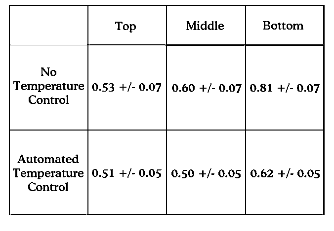
Table I. Post Deposition Drift (%)
Plasma Assisted Deposition
Plasma and ion assisted deposition are well-known methods10 which provide a means of imparting energy to the growing film, thereby modifying the microstructure to provide dense, near stoichiometric, films that are impervious to temperature and humidity variations.
The extent of film densification is dependent upon ion energy and ion to adatom arrival rate. This is demonstrated in Figure 10, which shows TiO2 refractive index as a function of ion current density and demonstrates that there is a threshold value above which the refractive index variation is minimal.
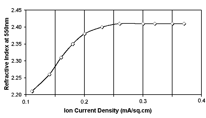
Figure 10. Refractive Index v. Ion Current Density.
As ion current density can vary across the coating area, in particular reducing with radial distance from the axis of the plasma/ion source, possible refractive index variation across the coating area is possible should the ion current density fall below the critical threshold value for a specific set of coating run conditions.
A means of automated control and monitoring of the ion current density is provided by using spatially distributed quartz crystals. On exposure to the ion current, the surface metal is etched at a measurable rate that can be related to an ion current density value, as measured using a Faraday cup. Typically, for Au coated crystals, etch rates of 2Å/sec/mA/cm2 of ion current density are observed (Ion energy approximately 100eV).
Therefore, etch rate output from the distributed quartz crystals provides a measure of the ion current density distribution and hence verification that the ion current density threshold to achieve constant refractive index is achieved.
CONCLUSIONS
Benefits of automated control of key process parameters - specifically thickness monitoring, spatial distribution of evaporant plume via multi-point quartz crystal monitoring and plasma source conditions - have been demonstrated. The concept of identifying and maximising a production tolerance at the design stage of optical coating manufacture greatly reduces development timescales and increases production yield. Plant operating variables have to be categorised with respect to optical property variations and necessary automated control of relevant process parameters implemented. To date, complex filters have been produced using this production approach with production tolerances of less than ±0.1%.
REFERENCES

Contact details:
Satis RTC Photonics Systems
Tel. + 44 (0)1767 313067
This page last updated on November 23rd. 2000 and is © Satis RTC Photonics Systems Y2000
Turnpike Farm
Potton Road
Biggleswade
Bedfordshire
SG18 0EP
England
Fax.+ 44 (0)1767 600331
Eml. sales@satisrtc.com